[1] Counter
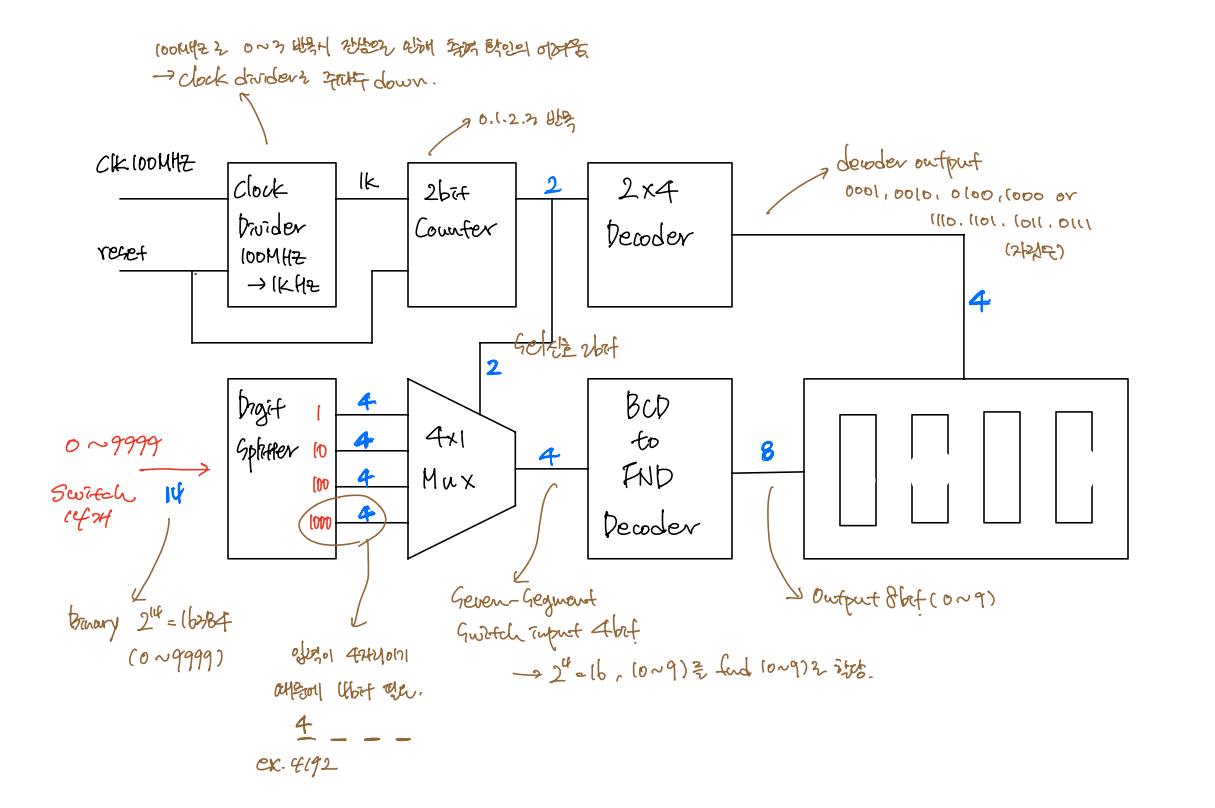
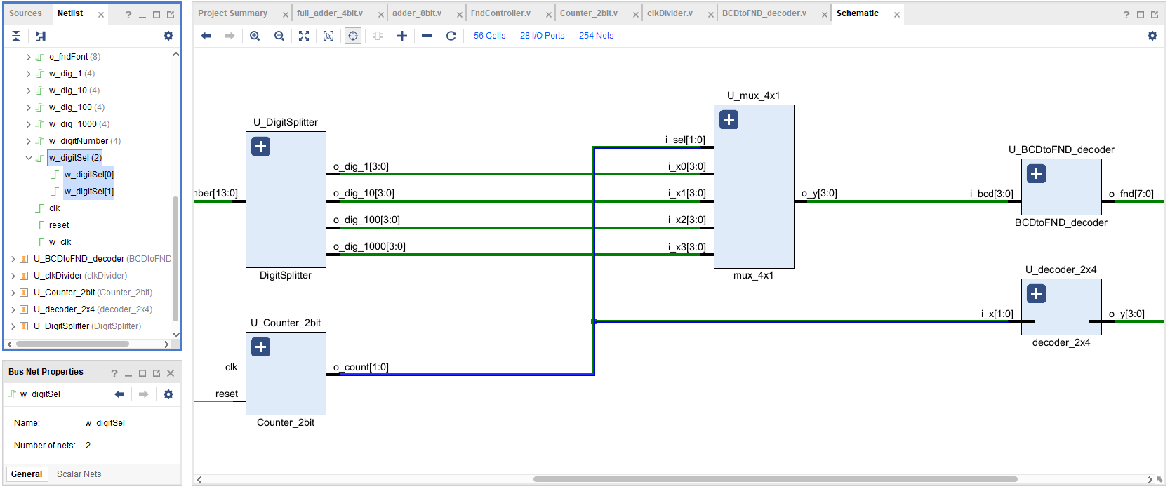
2x4 Decoder 의 출력 ([3:0] o_digitSel) 을 반복적으로 Count 하는 Counter 를 설계하려고 한다. 4 개의 7-Segment 를 동작하기 위해 Counter 의 bit 는 2-bit 이다. clk 가 들어올 때마다 + 1 씩 Count 가 쌓이게 되고, reset 입력 시, 0 으로 초기화 된다. Counter 의 출력 (o_count) 은 2x4 Decoder 의 입력 (i_x) 으로 들어간다.
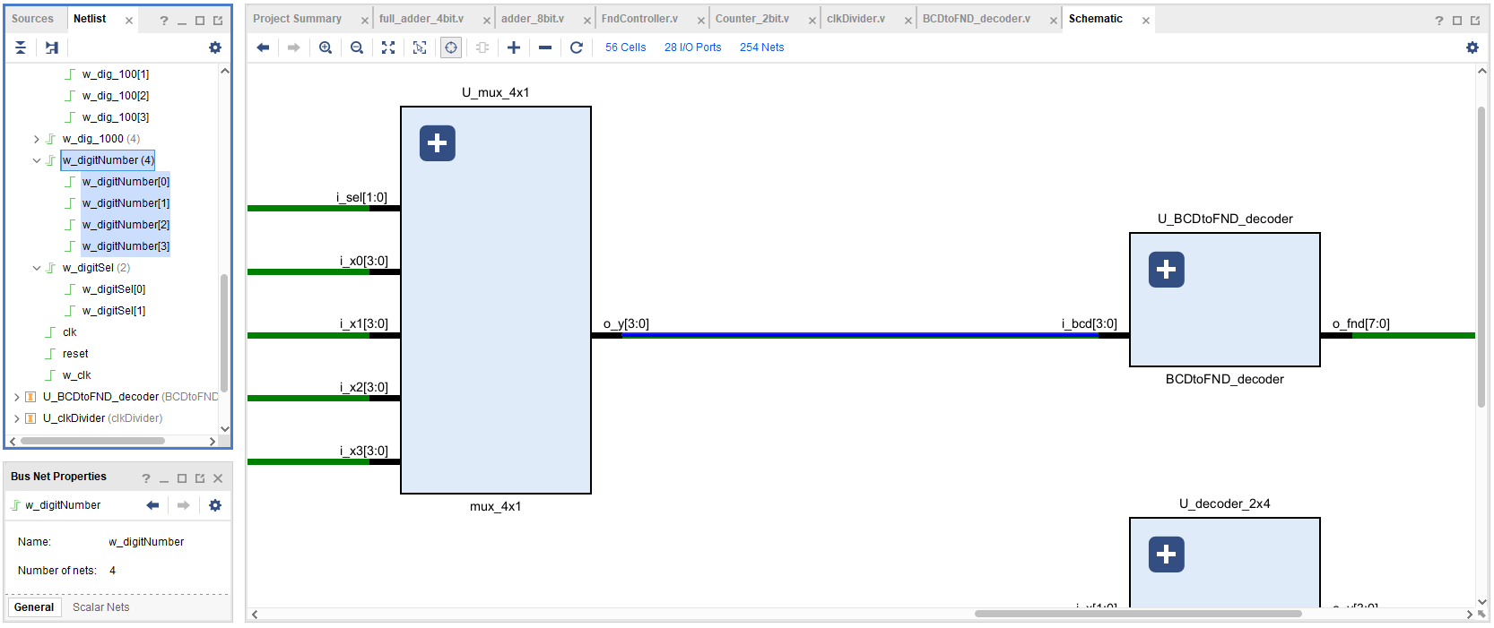
[2] DigitSplitter, mux 4x1
0 ~ 9999 사이의 값을 입력 ([13:0] i_number, 0 ~ 16384) 으로 받을 경우, 각 자릿 수의 [3:0] Digit Number (o_dig_1, o_dig_10, o_dig_100, o_dig_1000) 가 7-Segment LED (o_fndFont) 로 출력되어야 한다. 예를 들어, 입력 (i_number) 으로 4192 가 들어온다면 o_dig_1 : 0002, o_dig_10 : 0090, o_dig_100 : 0100, o_dig_1000 : 4000 으로 4-bit 씩 들어가고, 4x1 mux 를 통과한 출력 또한 4192, 4-bit 로 BCD to FND Decoder 의 입력 (i_bcd) 으로 들어간다.
[3] clkDivider
Basys-3 Board 를 사용하여 기본적으로 100Mhz 의 clk 을 입력으로 받음. 하지만 7-Segment LED 가 100Mhz 의 clk 을 받을 경우, 주파수가 높기 때문에 이전 출력의 잔상이 남아 정확한 출력 값을 확인하기 어려워진다. 잔상이 생기지 않고 정확한 출력 값을 확인하기 위해 clkDivider 를 거쳐 주파수를 낮추는 과정이 필요하다.
[1] Counter_2bit
`timescale 1ns / 1ps

module Counter_2bit(
    input clk,
    input reset,
    output [1:0] o_count
    );

    reg [1:0] r_counter = 2'b0;
    assign  o_count = r_counter;

    always@(posedge clk, posedge reset) begin
        if(reset) begin
            r_counter <= 2'b0;
        end
        else begin
            r_counter <= r_counter + 1;
        end
    end
endmodule
[2] DigitSplitter, 4x1 mux
`timescale 1ns / 1ps

module digitsplitter(
    input [13:0] i_number,
    output [3:0] o_dig_1,
    output [3:0] o_dig_10,
    output [3:0] o_dig_100,
    output [3:0] o_dig_1000
    );

    assign o_dig_1 = i_number % 10;
    assign o_dig_10 = i_number / 10 % 10;
    assign o_dig_100 = i_number / 100 % 10;
    assign o_dig_1000 = i_number / 1000 % 10;

endmodule
`timescale 1ns / 1ps
module mux_4x1(
input [1:0] i_sel,
input [3:0] i_x0,
input [3:0] i_x1,
input [3:0] i_x2,
input [3:0] i_x3,
output [3:0] o_y
);
reg [3:0] o_y;
always@(*) begin
case(i_sel)
2'b00 : o_y = i_x0;
2'b01 : o_y = i_x1;
2'b10 : o_y = i_x2;
2'b11 : o_y = i_x3;
default : o_y = 4'b0;
endcase
end
endmodule
[3] clkDivider 100Mhz - 1Khz
`timescale 1ns / 1ps

module clkDivider (
    input i_clk,
    input i_reset,
    output o_clk
);
    parameter N = 50_000;
    reg r_clk = 0;
    reg [32:0] r_counter = 0;

    assign o_clk = r_clk;

    always @(posedge i_clk, posedge i_reset) begin
        if(i_reset) begin
            r_counter <= 0;
            r_clk <= 0;
        end
        else begin
            if(r_counter == N - 1) begin // 1kHz
                r_counter <= 0;
                r_clk <= ~r_clk; // high -> low, low -> high toggle
            end else begin
                r_counter <= r_counter+1;
            end
        end

    end

endmodule

/*
module clkDivider (
    input clk, // 100MHz
    input reset,
    output reg o_clk=0 // 1KHz
    );
    reg [16:0] r_counter = 0;

    always @(posedge clk, posedge reset) begin // Comparing, Not Toggle
        if (reset) begin
            r_counter <= 0;
        end
        else begin
            if (r_counter == 100_000-1) begin
                r_counter <= 0;
                o_clk <= 1'b1;
            end
            else begin
                r_counter <= r_counter + 1;
                o_clk <= 1'b0;
            end
        end
    end
endmodule
*/
FndController Verilog Code
`timescale 1ns/1ps

module FndController (
    input clk,
    input reset,
    input [13:0] i_sw_bcd,
    output [3:0] o_digitSel,
    output [7:0] o_fndFont
);
    wire [1:0] w_digitSel;
    wire [3:0] w_digitNumber;
    wire [3:0] w_dig_1, w_dig_10, w_dig_100, w_dig_1000;
    wire w_clk;

    clkDivider U_clkDivider(
        .i_clk(clk),
        .i_reset(reset),
        .o_clk(w_clk)
    );

    Counter_2bit U_Counter_2bit(
        .clk(w_clk),
        .reset(reset),
        .o_count(w_digitSel)
    );

    decoder_2x4 U_decoder_2x4(
        .i_x(w_digitSel),
        .o_y(o_digitSel)
    );

    DigitSplitter U_DigitSplitter(
        .i_number(i_sw_bcd),
        .o_dig_1(w_dig_1),
        .o_dig_10(w_dig_10),
        .o_dig_100(w_dig_100),
        .o_dig_1000(w_dig_1000)
    );

    mux_4x1 U_mux_4x1(
        .i_sel(w_digitSel),
        .i_x0(w_dig_1),
        .i_x1(w_dig_10),
        .i_x2(w_dig_100),
        .i_x3(w_dig_1000),
        .o_y(w_digitNumber)
    );

    BCDtoFND_decoder U_BCDtoFND_decoder(
        .i_bcd(w_digitNumber),
        .o_fnd(o_fndFont)
    );


endmodule
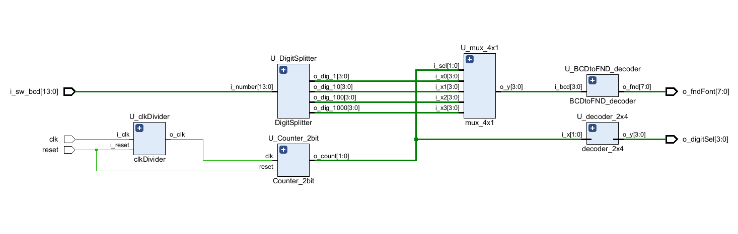
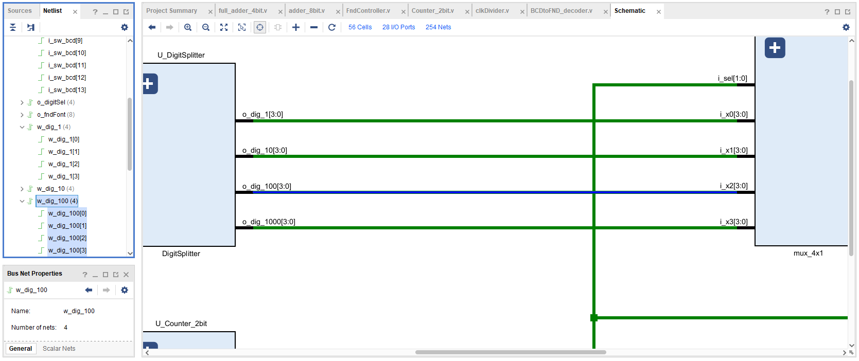
FndController 라는 상위 모듈 내의 U_clkDivider, U_counter_2bit, U_ DigitSlpitter 등과 같은 하위 모듈에서는 wire 선언을 통해 input / output port 를 서로 연결한다.
[4] Basys3 Board 에 Hard-ware I/O 를 연결.
## Clock signal
set_property -dict { PACKAGE_PIN W5   IOSTANDARD LVCMOS33 } [get_ports { clk }]; #IO_L12P_T1_MRCC_34 ,Sch=CLK100MHZ
create_clock -add -name sys_clk_pin -period 10.00 -waveform {0 5} [get_ports clk]


##Switches

set_property -dict { PACKAGE_PIN V17  IOSTANDARD LVCMOS33 } [get_ports { i_sw_bcd[0] }]; #IO_L19N_T3_A09_D25_VREF_14 ,Sch=SW0
set_property -dict { PACKAGE_PIN V16  IOSTANDARD LVCMOS33 } [get_ports { i_sw_bcd[1] }]; #IO_L19P_T3_A10_D26_14      ,Sch=SW1
set_property -dict { PACKAGE_PIN W16  IOSTANDARD LVCMOS33 } [get_ports { i_sw_bcd[2] }]; #IO_L20P_T3_A08_D24_14      ,Sch=SW2
set_property -dict { PACKAGE_PIN W17  IOSTANDARD LVCMOS33 } [get_ports { i_sw_bcd[3] }]; #IO_L20N_T3_A07_D23_14      ,Sch=SW3
set_property -dict { PACKAGE_PIN W15  IOSTANDARD LVCMOS33 } [get_ports { i_sw_bcd[4] }]; #IO_L21N_T3_DQS_A06_D22_14  ,Sch=SW4
set_property -dict { PACKAGE_PIN V15  IOSTANDARD LVCMOS33 } [get_ports { i_sw_bcd[5] }]; #IO_L21P_T3_DQS_14          ,Sch=SW5
set_property -dict { PACKAGE_PIN W14  IOSTANDARD LVCMOS33 } [get_ports { i_sw_bcd[6] }]; #IO_L22N_T3_A04_D20_14      ,Sch=SW6
set_property -dict { PACKAGE_PIN W13  IOSTANDARD LVCMOS33 } [get_ports { i_sw_bcd[7] }]; #IO_L22P_T3_A05_D21_14      ,Sch=SW7
set_property -dict { PACKAGE_PIN V2   IOSTANDARD LVCMOS33 } [get_ports { i_sw_bcd[8] }]; #IO_L5P_T0_34               ,Sch=SW8
set_property -dict { PACKAGE_PIN T3   IOSTANDARD LVCMOS33 } [get_ports { i_sw_bcd[9] }]; #IO_L2N_T0_34               ,Sch=SW9
set_property -dict { PACKAGE_PIN T2   IOSTANDARD LVCMOS33 } [get_ports { i_sw_bcd[10] }]; #IO_L1N_T0_34              ,Sch=SW10
set_property -dict { PACKAGE_PIN R3   IOSTANDARD LVCMOS33 } [get_ports { i_sw_bcd[11] }]; #IO_L2P_T0_34             ,Sch=SW11
set_property -dict { PACKAGE_PIN W2   IOSTANDARD LVCMOS33 } [get_ports { i_sw_bcd[12] }]; #IO_L5N_T0_34              ,Sch=SW12
set_property -dict { PACKAGE_PIN U1   IOSTANDARD LVCMOS33 } [get_ports { i_sw_bcd[13] }]; #IO_L3N_T0_DQS_34          ,Sch=SW13
#set_property -dict { PACKAGE_PIN T1   IOSTANDARD LVCMOS33 } [get_ports { i_b[6] }]; #IO_L3P_T0_DQS_34               ,Sch=SW14
#set_property -dict { PACKAGE_PIN R2   IOSTANDARD LVCMOS33 } [get_ports { i_b[7] }]; #IO_L1P_T0_34                   ,Sch=SW15
##7 segment display
set_property -dict { PACKAGE_PIN W7 IOSTANDARD LVCMOS33 } [get_ports { o_fndFont[0] }]; #IO_L13P_T2_MRCC_34 ,Sch=CA
set_property -dict { PACKAGE_PIN W6 IOSTANDARD LVCMOS33 } [get_ports { o_fndFont[1] }]; #IO_L13N_T2_MRCC_34 ,Sch=CB
set_property -dict { PACKAGE_PIN U8 IOSTANDARD LVCMOS33 } [get_ports { o_fndFont[2] }]; #IO_L14P_T2_SRCC_34 ,Sch=CC
set_property -dict { PACKAGE_PIN V8 IOSTANDARD LVCMOS33 } [get_ports { o_fndFont[3] }]; #IO_L14N_T2_SRCC_34 ,Sch=CD
set_property -dict { PACKAGE_PIN U5 IOSTANDARD LVCMOS33 } [get_ports { o_fndFont[4] }]; #IO_L16P_T2_34 ,Sch=CE
set_property -dict { PACKAGE_PIN V5 IOSTANDARD LVCMOS33 } [get_ports { o_fndFont[5] }]; #IO_L16N_T2_34 ,Sch=CF
set_property -dict { PACKAGE_PIN U7 IOSTANDARD LVCMOS33 } [get_ports { o_fndFont[6] }]; #IO_L19P_T3_34 ,Sch=CG
set_property -dict { PACKAGE_PIN V7 IOSTANDARD LVCMOS33 } [get_ports { o_fndFont[7] }]; #IO_L19N_T3_VREF_34 ,Sch=DP
set_property -dict { PACKAGE_PIN U2 IOSTANDARD LVCMOS33 } [get_ports { o_digitSel[0] }]; #IO_L9N_T1_DQS_34 ,Sch=DP
set_property -dict { PACKAGE_PIN U4 IOSTANDARD LVCMOS33 } [get_ports { o_digitSel[1] }]; #IO_L11P_T1_SRCC_34 ,Sch=DP
set_property -dict { PACKAGE_PIN V4 IOSTANDARD LVCMOS33 } [get_ports { o_digitSel[2] }]; #IO_L11N_T1_SRCC_34 ,Sch=DP
set_property -dict { PACKAGE_PIN W4 IOSTANDARD LVCMOS33 } [get_ports { o_digitSel[3] }]; #IO_L12N_T1_MRCC_34 ,Sch=DP
##Buttons
set_property -dict { PACKAGE_PIN U18 IOSTANDARD LVCMOS33 } [get_ports { reset }]; #IO_L18N_T2_A11_D27_14 ,Sch=BTNC
#set_property -dict { PACKAGE_PIN T18 IOSTANDARD LVCMOS33 } [get_ports { i_pbstoprun }]; #IO_L17N_T2_A13_D29_14 ,Sch=BTNU
#set_property -dict { PACKAGE_PIN W19 IOSTANDARD LVCMOS33 } [get_ports { btnL }]; #IO_L16N_T2_A15_D31_14 ,Sch=BTNL
#set_property -dict { PACKAGE_PIN T17 IOSTANDARD LVCMOS33 } [get_ports { btnR }]; #IO_L17P_T2_A14_D30_14 ,Sch=BTNR
#set_property -dict { PACKAGE_PIN U17 IOSTANDARD LVCMOS33 } [get_ports { i_pbclear }]; #IO_L18P_T2_A12_D28_14 ,Sch=BTND'[Harman] 반도체 설계 > Vivado' 카테고리의 다른 글
| [Vivado] 06. Calculator 8bit, FSM StopWatch 0.1s UpCount (0) | 2023.08.05 |
|---|---|
| [Vivado] 05. Finite State Machine LED (0) | 2023.08.05 |
| [Vivado] 04. FndController, Adder 8bit (0) | 2023.08.05 |
| [Vivado] 03. Adder 8bit (0) | 2023.08.05 |
| [Vivado] 01. FndController, 2x4_Decoder (0) | 2023.08.04 |


