Logic Gate, NOT
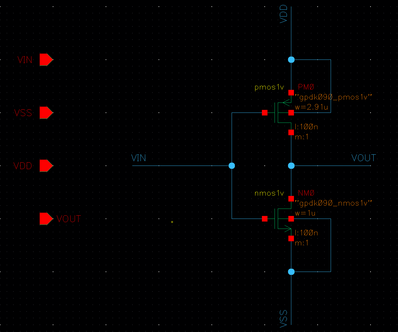
N-MOS 하나와 P-MOS 하나로 이루어진 NOT Gate 의 Circuit 형태는 다음과 같다.

P-MOS 와 N-MOS 의 Body 는 Source 와 연결되어 각각 VDD, VSS(GND) 로 이어진다.
Fig 10.59 에서 Body 는 생략.

Create - Instance, 단축키 I

Image 를 드래그해서 Schematic 창으로 가져옴.
클릭 안해도 됨.
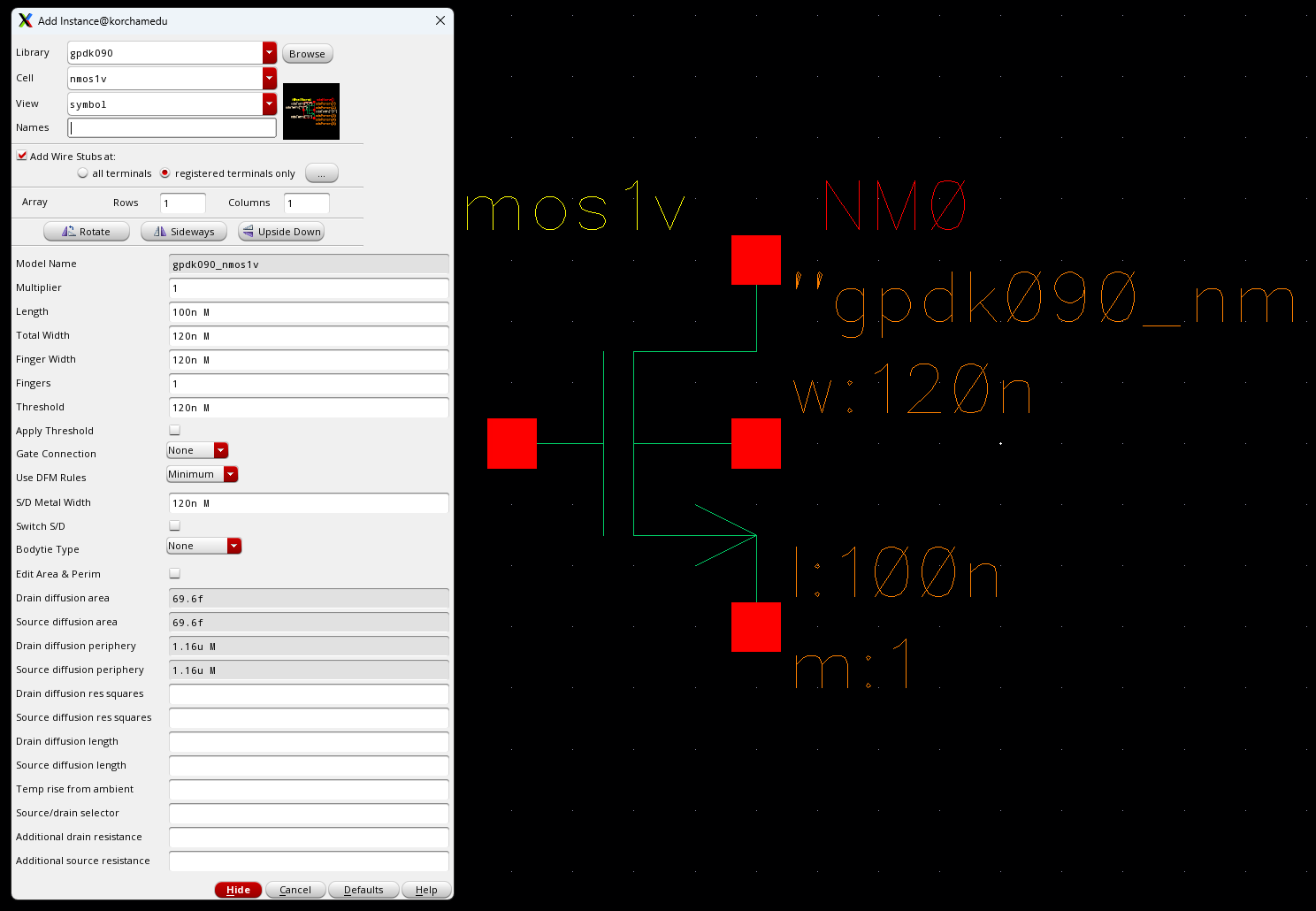
N-MOS

P-MOS

Fig 10.59 처럼 P-MOS 의 Body, Source 는 VDD 로, N-MOS 의 Body, Source 는 VSS(GND) 로 연결한다.
Pin, Label 추가.
Pin 과 Label 은 연결되어 있음.
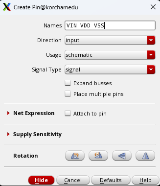
VOUT 은 Direction 을 output 으로 설정.

Schematic 이 끝났으면 Check and save.
virtuoso log 창에서 "Schematic check completed with no errors." 확인.
'[Harman] 반도체 설계 > Full Custom IC' 카테고리의 다른 글
| Full Custom IC - Logic Gate Lay-out. (0) | 2023.07.09 |
|---|---|
| Full Custom IC - Logic Gate Schematic & Simulation Results. (0) | 2023.07.09 |
| Full Custom IC - Logic Gate Simulation. (0) | 2023.07.09 |
| Full Custom IC - Logic Gate Symbol. (0) | 2023.07.09 |
| Full Custom IC - Virtuoso. (0) | 2023.07.08 |


